It has been almost 60 years since the Feynman’s famous lecture “There’s plenty of room at the bottom” [1]. In his paper, he asked, "How do we write small?" The same question is still asked today. Although the techniques have moved forward since the 1960s and the linewidths used in the semiconductor industry have gone down drastically, we are still looking for methods to produce small structures with high-throughput.
Photolithography techniquesThe most used patterning technique is called photolithography. In photolithography, a pattern on the 2D mask is transferred to a substrate with the help of photoresist and UV-light. Different photolithography systems can be divided according to the wavelengths used, for example, UV- and X-ray lithography.
In research laboratories, the most common patterning method is UV-lithography. This method utilizes UV-light, with a wavelength of around 400 nm. As the wavelength used, partly determines the minimum linewidth, shorter wavelengths are needed to produce smaller structures. Deep UV-lithography utilizes lasers with down to 193 nm wavelength and can produce below 50 nm features. Extreme UV (13.5 nm) and X-rays have also been tried out. Deep UV, extreme UV, and X-ray methods can create structures in nanometer scale, but they are expensive due to instruments cost. Special requirements set for photomasks and photoresists used also increase the costs and complexity of the methods.
Another commonly used method in research laboratories for nanostructure fabrication is electron beam (e-beam) lithography. In e-beam lithography, a photoresist is again used to transfer the structures to the underlying substrate, but instead of using the laser to pattern the photoresist, a focused electron beam is utilized. The main advantage of the e-beam lithography is high resolution with sub 10 nm patterns. As direct writing produces the pattern, the method is very slow and usually used to pattern small areas.
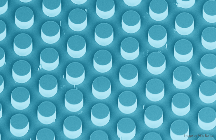
A third method, described here, is nanosphere lithography. Here, nanoparticles are deposited on the substrate, and the pattern is transferred by using the nanospheres as an etching mask. The size of the nanoparticles defines the pattern resolution. Nanosphere lithography is an inexpensive and potentially high-throughput fabrication method for a regular array of nanosized features. The most critical step is the fabrication of the colloidal crystal mask, which requires highly controlled nanoparticle deposition.
If you want to read more about how to deposit the nanoparticles, please download a short review titled “5 most common nanoparticle deposition methods”.

Susanna is an Application Scientist at Biolin Scientific. In her PhD thesis, she developed fabrication methods for a new type of inorganic-organic polymers. Microfabricated polymer chips were utilized as tool for biomolecule separation in analytical chemistry.